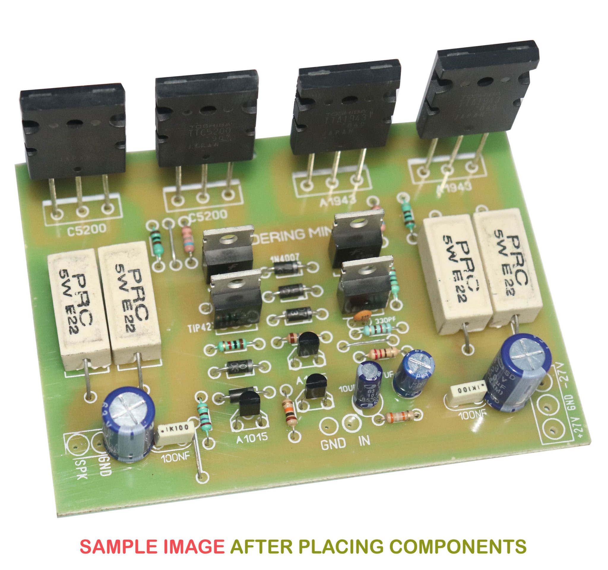
Pcb Layout 2sc5200 2sa1943 Amplifier Circuit Diagram Pdf
This is the voltage the amplifier needs from the power supply to get the desired output power. To find the maximum supply voltage, take the peak output voltage and add the voltage drop (Vod) of the LM3886 (4 V). Then factor in your transformer's regulation and the variation in your mains voltage.
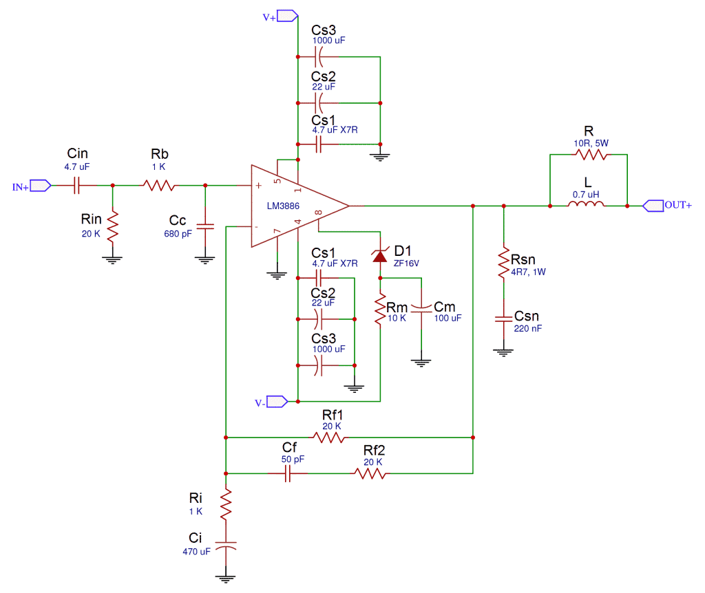
A Complete Guide to Design and Build a HiFi LM3886 Amplifier Circuit
The significance of a thoughtfully crafted PCB layout for audio amplifiers cannot be overstated. Just like a conductor directing a grand orchestra, the layout of the PCB can profoundly impact the performance, efficiency, and sound quality of the amplifier it supports. A well-designed PCB ensures optimal signal flow, minimizes interference.
New Audio Amplifier Circuit Diagram With Layout Pdf Wiring Digital
Amplifier Layout Gyunam Jeon, Yixuan He, Yong-Bin Kim This tutorial briefly introduces the circuit simulation in Cadence. A simple common-source amplifier has been built and simulated step by step using layout entry. Layout 1. Open Existing Schematic o Select ^File _ in IW → ^Open to open the existing schematic (Ex: CS_AMP) ..
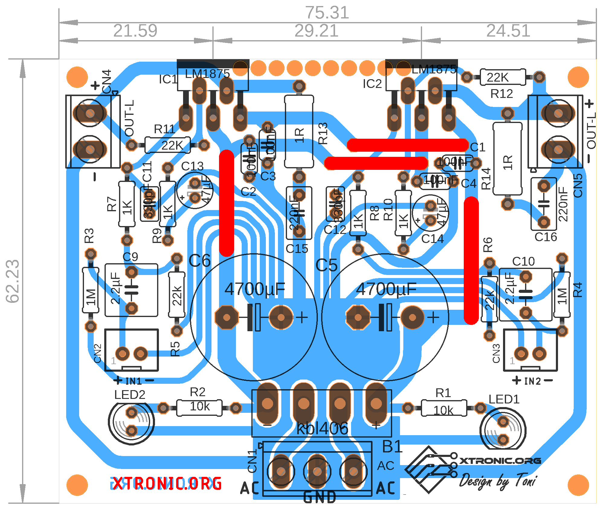
Lm1875stereopoweramplifiercircuitlayout
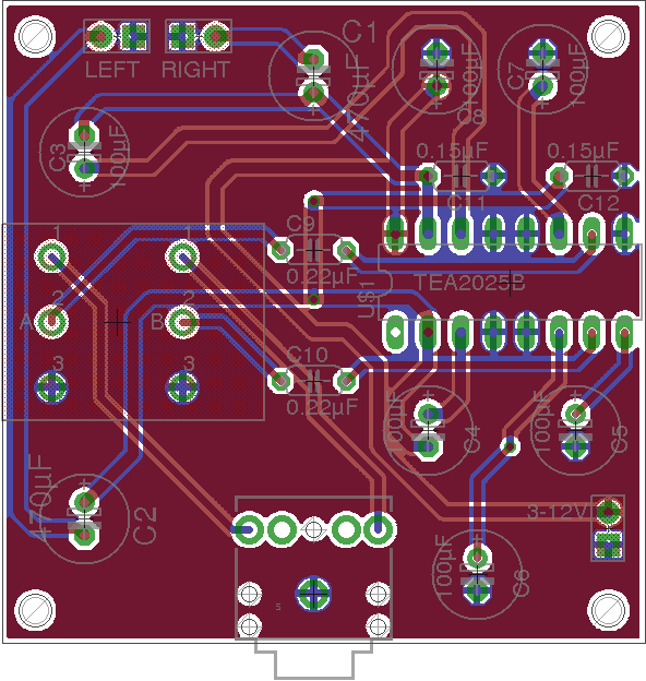
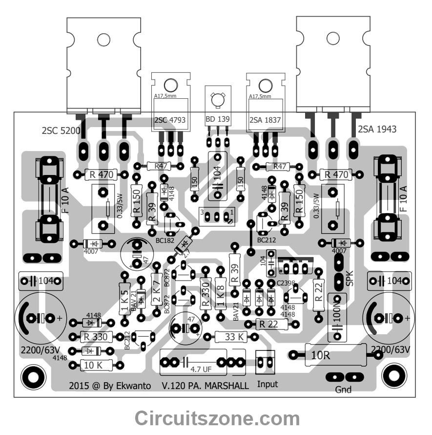
More Circuit, PCB layout! This just shares PCB Power Amplifier, Tone Control Speaker Protector, etc. You can see all about PCB Design from all around the world here, please wait until all PCB image appear's: PCB Power Amplifier OCL Garpendoz: PCB Power Amplifier APEX AX6: PCB Power Amp APEX AX11. PCB Power Apex AX11-MK2. PCB Power Amplifier AX14.
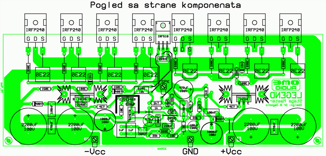
250W RMS Power Amplifier Legend Stage Master Circuit Scheme
The core of this CMOS power amplifier design tutorial: transistor networks come down to series and parallel configurations. Modern electronics rely on amplifier networks to boost voltage, current, or power signals to appreciable levels for further use. Instead of using high voltage or current signals directly from a source that could impact.
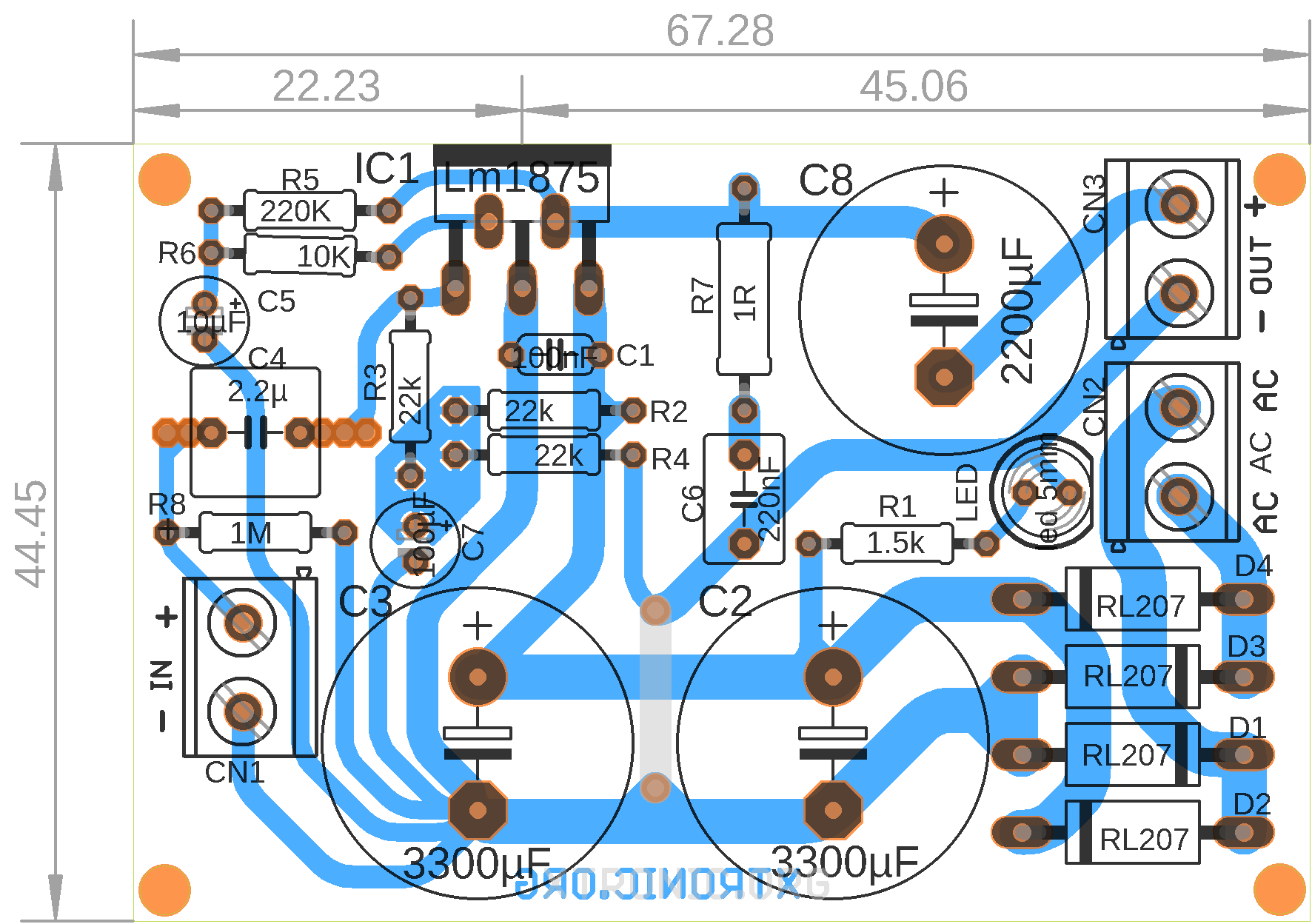
Circuit Of Power Audio Amplifier Lm1875 20W
OPAMP Layout Project files in GitHubhttps://github.com/rhovector/Cadence_Virtuoso_180nm_Projects1. Layout design for OpAmp in 180nm2. Verification of DRC and.

layout pcb amplifier Simple Micro amp BLOGKAMARKU
How to Build an LM1875 Audio Amplifier. We are going to design and build an amplifier based on the LM1875 amplifier chip. Here's a pin diagram of the LM1875: LM1875 Pinouts. The circuit is fairly simple. It's the same schematic included in the LM1875 datasheet: LM1875 from TI datasheet, dual power supply version.

Amplifier Pcb Layout, Power Amplifier Pcb Layout Expert Manufacturer
PCB layout of Amplifier. A graphic drawing of copper wire designs performed on a circuit board is an amplifier printed circuit board layout. A PCB builder achieves this. This mechanism allows the Amplifier PCB to boost the amount of input signal loaded into it. Amplifier PCB can be used in several applications.
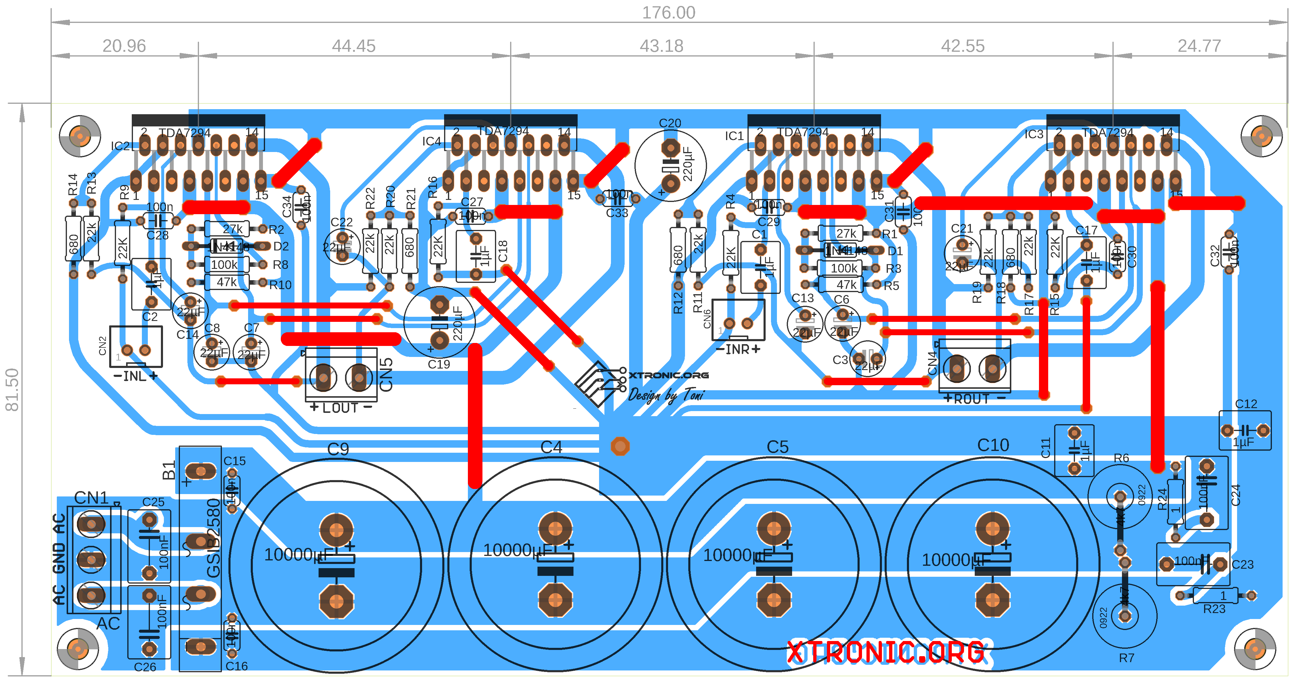
Tda7294_bridge_layout_amplificador
the op amp's place in the world of analog electronics. Chapter 2 reviews some basic phys-ics and develops the fundamental circuit equations that are used throughout the book. Similar equations have been developed in other books, but the presentation here empha-sizes material required for speedy op amp design. The ideal op amp equations are devel-
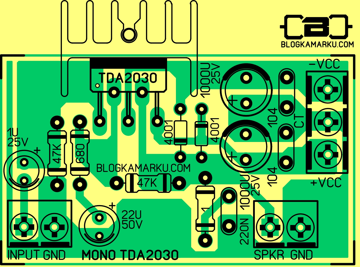
PCB Layout Power Amplifire TDA 2030 Versi standard BLOGKAMARKU
The Ground's Connections in Amplifier PCB. The ground plane should be connected to both of the device's ground pins as tightly as feasible. To prevent multiple ground loops from forming, all unit grounds should be shorted. A direct connection from the unit pads to the ground plane prefers. 3.

Amplifier Circuit Diagram With Pcb Layout
Introduction of Amplifier PCB Layout. An audio amplifier is a circuit board that takes an audio signal from a system like a microphone or a loudspeaker receiver and amplifies it. To make an amplifier, you need a circuit layout that generates the input signal and improves the output. If you don't, you could have a lousy circuit configuration.

layout pcb amplifier Simple Micro amp BLOGKAMARKU
Venture amplifier PCB layout team has full experience in processing a wide variety of printed circuit board materials. Through our 2 hours rapid response services from our 24/7 sales and tech support team, and excellent after-sales service, we will be your expert amplifier PCB layout partner in China.

Amplifier Pcb Layout, Power Amplifier Pcb Layout Expert Manufacturer
Figure 5. Example Layout of Non Inverting Amplifier with Leakage Guard Ring. For low-leakage applications, the LTC2057 is available in an MS10 package with a special pinout that facilitates the layout of guard ring structures. The pins adjacent to the inputs have no internal connection, allowing a guard ring to be routed through them.
Layout amplifier
The layout could be improved, however, to reduce PCB parasitic impedances and optimize performance. The first improvement we made is moving R1 and R2 next to the inverting pin (pin 2) of the OPA191; this will help reduce stray capacitance on the inverting pin. The inverting pin of an op amp is a high-impedance node and is therefore "sensitive

350 Studio Amplifier Circuit Scheme and PCB Layout Amplifier Circuit
LAYOUT CONSIDERATIONS. There are many tried and true conventions for the layout of guitar amplifiers that have served the amp building community well. These are by no means the only way to successfully layout a design, but beginners are particularly encouraged to follow these conventions.

Power Amplifier Circuit Diagram With Pcb Layout Pdf Fannie Top
Amplifier design and layout can get much more complicated than component datasheets would have you believe. Anytime an amplifier is designed in terms of circuit design, physical layout, and PCB layout, amplifier stability should be an important consideration. There are times, however, when an amplifier is pushed to its limit and does not.